CH14: Advanced Physical Acquisition
Introduction
For most of the first decade of mobile forensics, three techniques defined what an examiner could pull from a locked or damaged phone: JTAG, In-System Programming (ISP), and chip-off acquisition. When a Nokia feature phone arrived in an evidence bag with a cracked screen and no PIN, an analyst with a RIFF Box, a steady hand, and the right pinout could read the raw NAND in an afternoon. Early Android handsets and pre-A7 iPhones were just as cooperative. Vendor tooling like Easy JTAG, Medusa Pro, Octoplus, and UFI Box turned what had been a research-grade procedure into a workflow a small lab could actually staff.
That world has narrowed for smartphones. Apple's introduction of the Secure Enclave Processor (SEP) with the A7 in 2013, followed by Android's broad adoption of File-Based Encryption (FBE) and dedicated security cores like Google's Titan M2 and the Tensor security core, changed the math. A perfect bit-for-bit dump of a modern smartphone's NAND is now well-organized ciphertext, bound to a hardware key the examiner cannot extract. Chip-off on a current iPhone or Pixel returns data the examiner cannot read.
The techniques themselves did not die. They migrated. Today they remain the workhorses of any investigation that touches Internet of Things (IoT) hardware, drones, automotive infotainment, body cameras, GPS units, fitness wearables, smart-home hubs, kiosks, and a long tail of embedded devices built to a price point that excluded a hardware-backed key store. They are also the last resort for physically damaged storage and for the legacy feature phones that still surface in elder-fraud and cold-case work.
This chapter closes the course by mapping the full physical acquisition spectrum, showing where each technique lives in 2026, and giving you the analytical framework to decide when invasive acquisition is the right call.
Learning Objectives
After completing this chapter, you will be able to:
- Distinguish JTAG, ISP, and chip-off acquisition by access point, invasiveness, and ideal use case.
- Explain why hardware-backed encryption on modern smartphones renders raw NAND dumps unrecoverable without the user credential.
- Identify the device classes (IoT, drones, automotive, wearables, GPS, kiosks, legacy phones) where physical acquisition remains the most viable path.
- Compare hot-air and cold (mechanical) chip removal in terms of risk, equipment, skill floor, and evidence preservation.
- Document the chain-of-custody, validation, and reporting steps unique to invasive acquisition.
14.1 The Physical Acquisition Spectrum
Mobile forensics arranges acquisition methods on a hierarchy from least to most invasive. Logical acquisition uses the device's own APIs to copy user-accessible data. File system acquisition copies the visible filesystem, often with elevated privileges. Physical acquisition captures the underlying storage at the block level, including unallocated space and deleted artifacts. Advanced physical acquisition sits at the top of that hierarchy. It bypasses the operating system entirely and reads the storage chip directly through hardware test points, soldered leads, or, in the most invasive case, after physically removing the chip from the board.
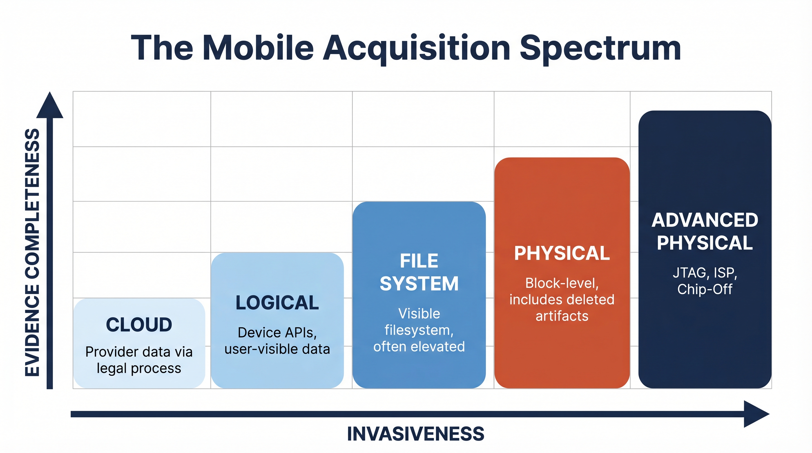
Figure 14.1: The mobile acquisition spectrum. As invasiveness increases, evidence completeness increases but reversibility and proportionality concerns rise sharply.
The three techniques in this chapter share a common goal of producing a raw NAND, eMMC, or Universal Flash Storage (UFS) image, but they differ sharply in how they get there. JTAG talks to the processor and asks it to read storage on the examiner's behalf. ISP bypasses the processor and talks directly to the storage chip while it remains soldered to the board. Chip-off removes the storage chip entirely and reads it in a bench-top adapter.
Analyst Perspective
Think of these methods as a graduated response. ISP is preferred over chip-off when the board is intact, because it preserves the device for later re-examination. Chip-off is reserved for cases where the board cannot be repaired or the chip cannot be reached in-system. The choice is rarely about what is technically possible. It is about what is proportionate to the case and what preserves the most evidentiary value.
A Brief History of NAND-Level Tooling
Before smartphones, the JTAG and chip-off ecosystem was dominated by GSM-era tooling. RIFF Box, originally a service tool for GSM repair shops, became a de facto JTAG flasher for forensic use. Medusa Pro, Z3X Easy JTAG, Octoplus, and UFI Box added support for newer chips and faster eMMC pinouts as Android storage standards stabilized. By the early 2010s, dedicated chip-off rigs and BGA (Ball Grid Array) socket adapters from vendors like Dataman and PRG turned chip reading into a repeatable, if slow, lab operation. Most of these vendors still ship hardware in 2026, though product lines have consolidated and the smartphone market they originally served has largely moved out of reach.
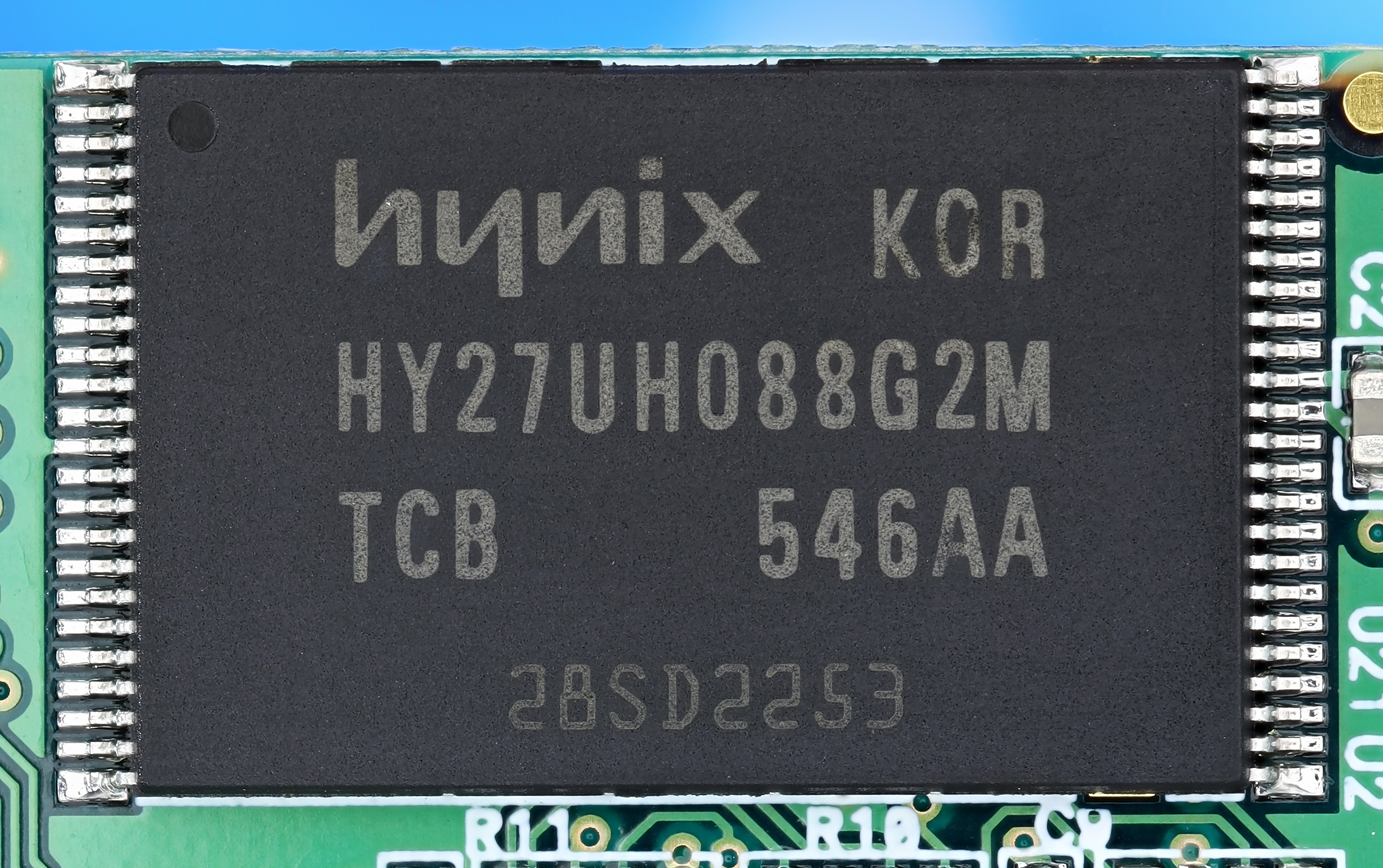
Figure 14.2: A discrete TSOP-48 NAND flash chip of the type that dominated feature-phone era chip-off work. Image by Mister rf, CC BY-SA 4.0 via Wikimedia Commons.
14.2 JTAG Acquisition
JTAG (Joint Test Action Group) is the colloquial name for IEEE Standard 1149.1, an industry standard originally designed to test printed circuit boards (PCBs) at the factory. The standard defines a small set of pins called the Test Access Port (TAP), through which an external tool can drive the device's processor into a controlled state, walk its internal registers, and instruct it to read or write attached memory. Forensic JTAG repurposes this debug interface to compel the processor to dump the contents of the NAND or eMMC chip it manages.
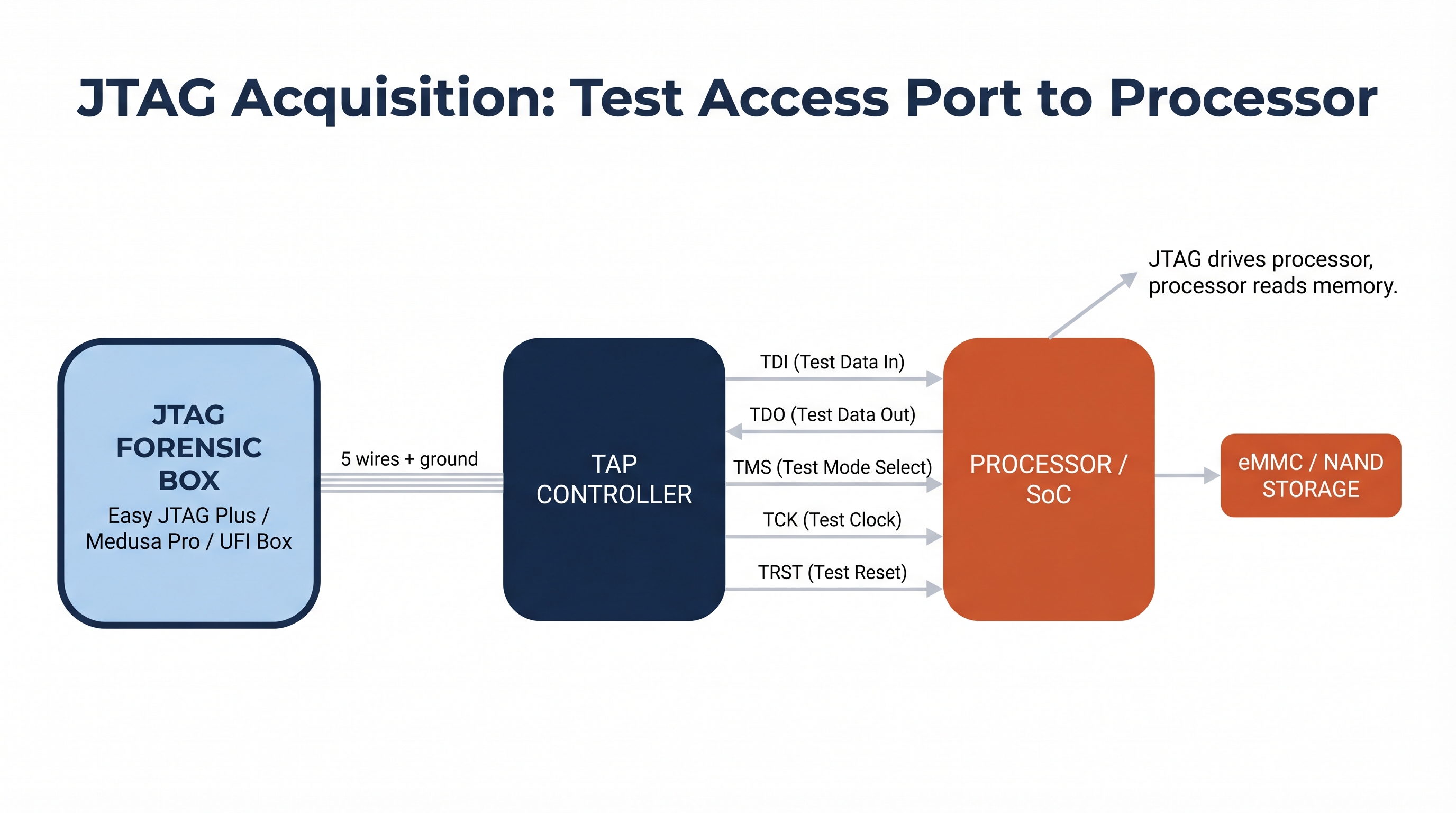
Figure 14.3: The JTAG acquisition path. The forensic box drives five signal wires into the processor's TAP, which then reads the storage chip on the examiner's behalf.
Acquiring data over JTAG requires four ingredients: the TAP pinout for the specific board, a JTAG-capable interface device (the "box"), a connection method (a soldered jig, spring-loaded pogo pins, or a vendor-supplied adapter), and a profile telling the box how to drive the target processor.

Figure 14.4: The IEEE 1149.1 TAP controller state machine. A JTAG forensic box drives this state machine through the TMS pin to load instructions and read or write memory through the target processor. Image by Rudolph H, free use via Wikimedia Commons.
The pinout is usually the hardest part. Vendor pinout databases such as those bundled with Easy JTAG Plus, Medusa Pro II, and the community-maintained GSMHosting and JTAG Test Points archives catalog tens of thousands of board variants. When a pinout is not in the database, the examiner must trace the test points by hand using a multimeter and a known JTAG box behavior, which can take hours per board.
JTAG's main advantages are non-destructive access and tolerance for moderate physical damage. A phone with a shattered screen and a dead USB port can often still respond on its TAP pads. Its main disadvantages are slow read speeds (often hours for a full eMMC dump) and dependence on a cooperating processor. If the processor is dead, JTAG is dead with it.
Analyst Perspective
JTAG is most valuable on lower-end Android devices, automotive infotainment heads, and embedded boards that still expose factory test pads. On modern flagships those pads have been removed or fused off, which is one of the reasons examiners moved to ISP for smartphone work.
14.3 ISP (In-System Programming) Acquisition
In-System Programming bypasses the processor entirely and speaks directly to the storage chip while it remains soldered to the board. For eMMC (embedded MultiMediaCard) storage, this means soldering fine wires to a defined set of pads: CMD (command), CLK (clock), DAT0 (data line zero), VCC (chip power), VCCQ (I/O power), and GND (ground). UFS storage uses a different pad set but the same principle. The wires lead to an ISP-capable reader, typically the same hardware used for JTAG (Easy JTAG Plus, Medusa Pro II, UFI Box, Z3X), running in a different mode.
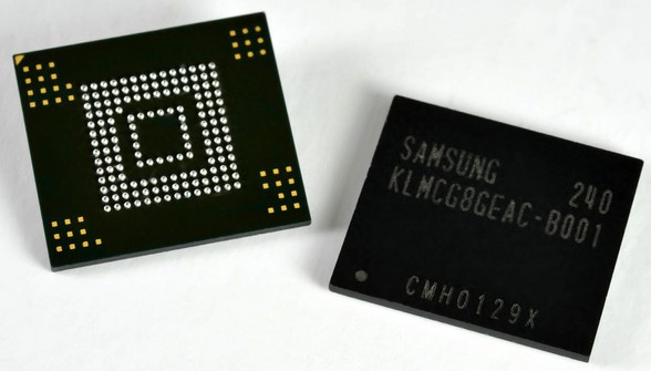
Figure 14.5: A Samsung eMMC memory chip showing the underside BGA pad layout. Only a small subset of these pads carry the data, clock, command, and power signals an ISP examiner needs to tap. Image by Toniperis, CC BY-SA 4.0 via Wikimedia Commons.
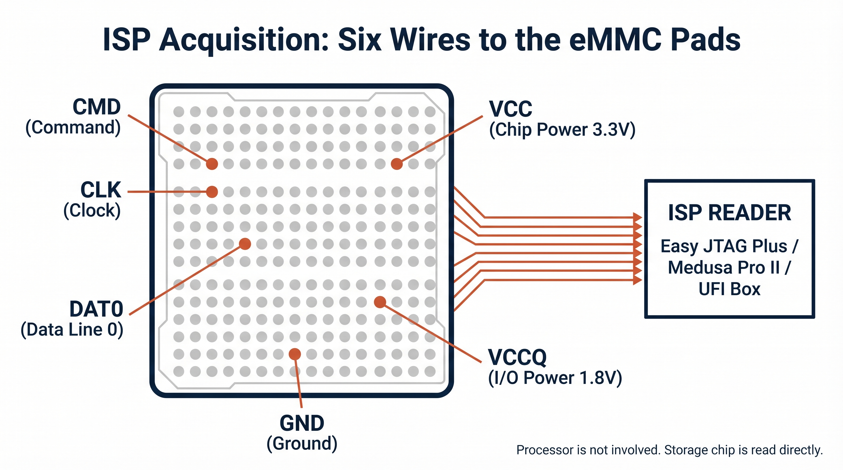
Figure 14.6: ISP wiring schematic. The examiner solders to six specific pads on the eMMC underside (out of dozens) and reads the chip directly through an ISP reader, bypassing the processor entirely.
ISP largely supplanted JTAG for smartphone work in the mid-2010s for three reasons. The eMMC pad layout is far more uniform across vendors than JTAG TAP locations. ISP does not require a working processor, so it survives processor-level damage that would block JTAG. Read speeds are also faster, often two to three times faster than JTAG on the same board.
The tradeoff is skill floor. ISP demands precise micro-soldering on pads that are often less than a millimeter apart, frequently buried under shielding cans that must be removed and replaced. A failed solder joint can short the chip and destroy the evidence. Most lab programs treat ISP as a competency requiring formal training, hours of supervised practice on scrap boards, and a peer-review step before touching evidence.
Warning
ISP looks deceptively similar to a repair-shop board rework, but the standards are not the same. A repair tech can replace a damaged board if a solder lifts a pad. A forensic examiner cannot. Every procedure must be planned, photographed, and reversible to the maximum extent possible. If you would not be willing to defend your soldering work in a deposition, you are not ready to perform ISP on evidence.
14.4 Chip-Off Acquisition
Chip-off is the most invasive option in the physical acquisition toolkit. The examiner physically removes the storage chip (eMMC, eMCP, UFS, or raw NAND) from the PCB, cleans it, and reads it in a bench-top adapter. Once removed, the chip can be re-read indefinitely, but the device itself is generally beyond reuse without a board-level repair.
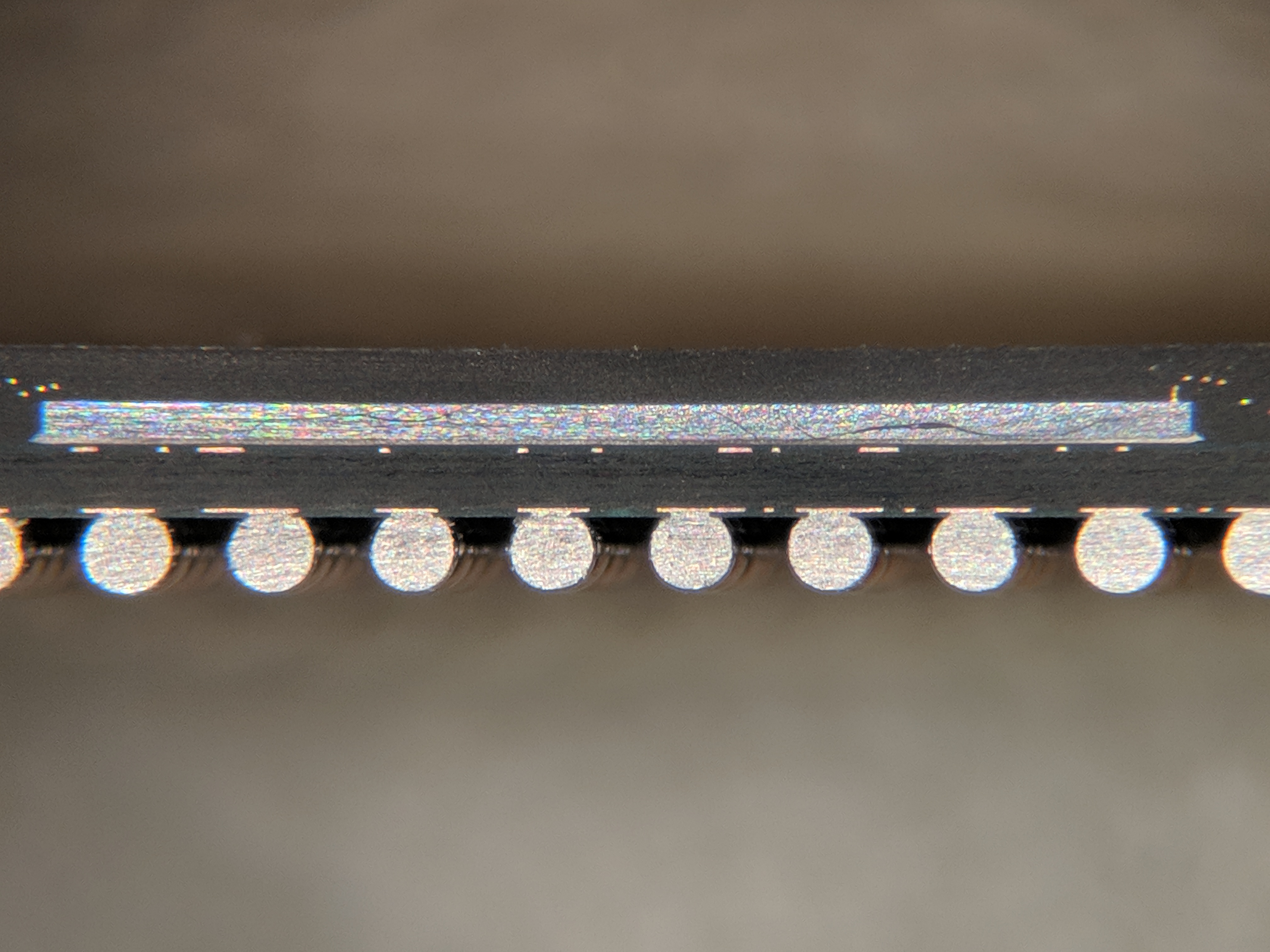
Figure 14.7: Cross-section of a BGA chip package, showing the silicon die on top and the row of solder balls connecting the package to the PCB beneath. Chip-off acquisition succeeds or fails on whether all of these connections can be released without harming the die. Image by TubeTimeUS, CC BY-SA 4.0 via Wikimedia Commons.
Two removal methods dominate, distinguished by whether they apply heat.
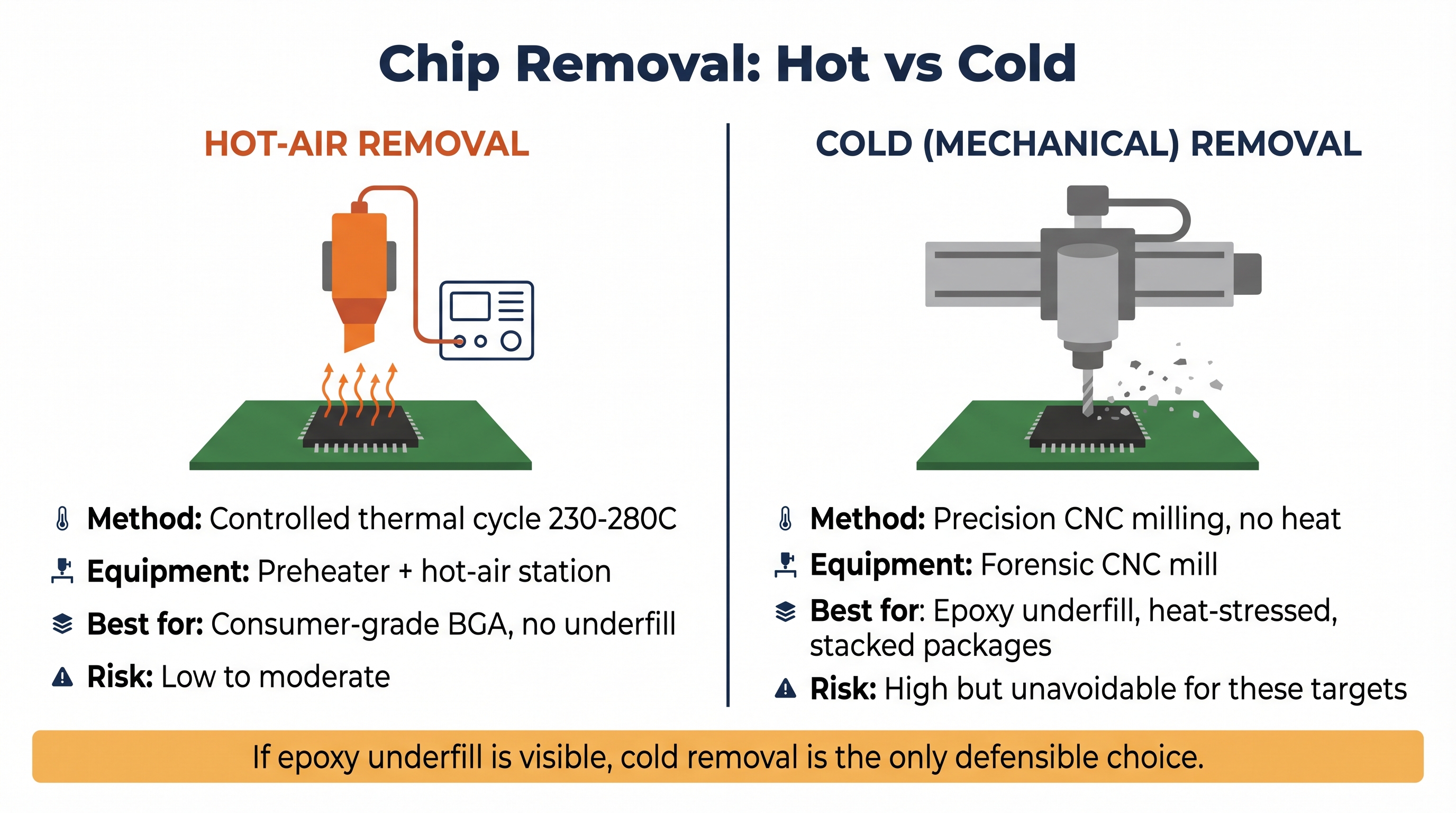
Figure 14.8: Hot-air and cold (mechanical) chip removal compared. The single most important decision factor is the presence of epoxy underfill or prior thermal stress.
14.4.1 Hot-Air Chip Removal
Hot-air chip-off uses a controlled thermal cycle to liquefy the solder balls under a BGA package so the chip can be lifted free. The workflow combines a board preheater (which brings the entire PCB to roughly 150 °C to prevent thermal shock) with a hot-air rework station (which delivers a focused stream at roughly 230 °C to 280 °C above the chip). Flux is applied to improve heat transfer and protect adjacent components. Once the solder reflows, the chip lifts off cleanly with vacuum tweezers.
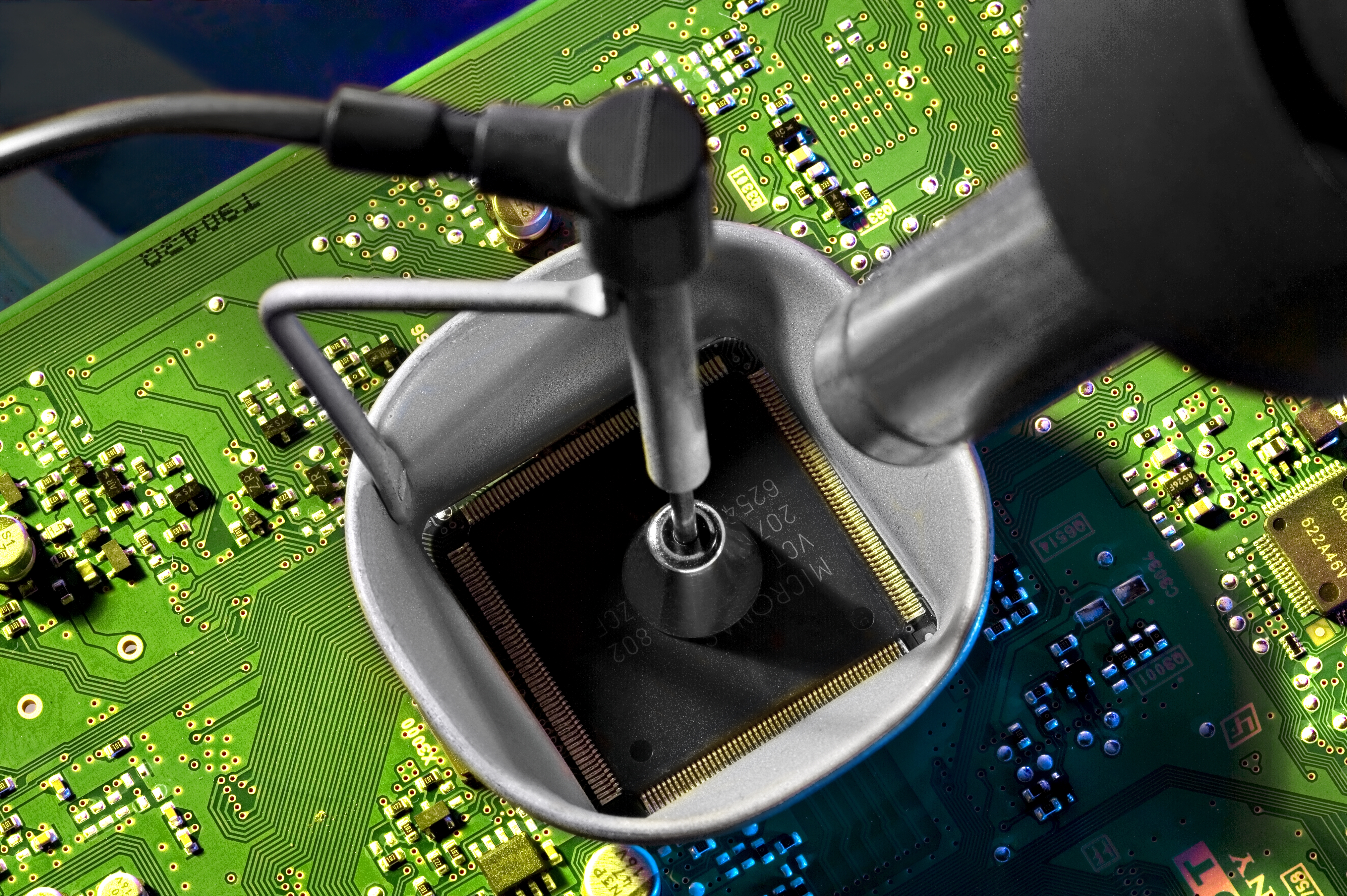
Figure 14.9: A hot-air rework station lifting a chip from a PCB. Forensic hot-air chip-off uses the same equipment paired with a board preheater for thermal control and a stereo microscope for placement. Image by Aisart, CC BY-SA 3.0 via Wikimedia Commons.
Removed chips are typically reballed (new solder balls applied to the package's pad grid) before being placed in a socket adapter such as the Dataman 48Pro2 with the appropriate BGA socket, the UP-828P programmer with eMMC socket modules, or the Easy JTAG socket family. The adapter presents the chip to the reader as if it were still in-circuit, and the reader produces the raw image.
The skill floor is high but not exotic. A trained examiner with a quality preheater, a temperature-controlled hot-air station, decent flux, a stereo microscope, and a reballing stencil can perform hot-air chip-off reliably on most consumer-grade BGA packages. The hard parts are consistency and patience.
14.4.2 Cold (Mechanical) Chip Removal
Cold chip-off removes the chip by mechanical means, usually with a precision CNC milling machine or a controlled grinding rig. There is no thermal cycle. The examiner mills away the PCB substrate under and around the chip until the package separates from the board, then cleans the underside and reads the chip in the same kind of socket adapter used for hot-air work.
Cold removal exists because some chips will not survive heat. Three situations are typical:
- Epoxy underfill. Many automotive, military, and industrial-grade boards are assembled with a structural epoxy under the BGA package to resist vibration. Heating an underfilled chip risks delaminating the package, cracking the silicon, or pulling the pads off when the chip is lifted.
- Already heat-stressed chips. A device recovered from a fire, a lithium thermal runaway, or a hot car may have a chip that survived the original event but cannot tolerate a second thermal cycle.
- Stacked or sandwiched packages. Some eMCP (embedded Multi-Chip Package) parts combine flash and RAM in one stack. A poorly controlled hot-air cycle can disturb the internal stack even if the package lifts cleanly.
Cold chip-off is slower (often a full shift per chip), demands more expensive equipment (a forensic-grade CNC mill costs in the tens of thousands of dollars), and carries less margin for error. The benefit is that it works on chips where any thermal approach would destroy the evidence.
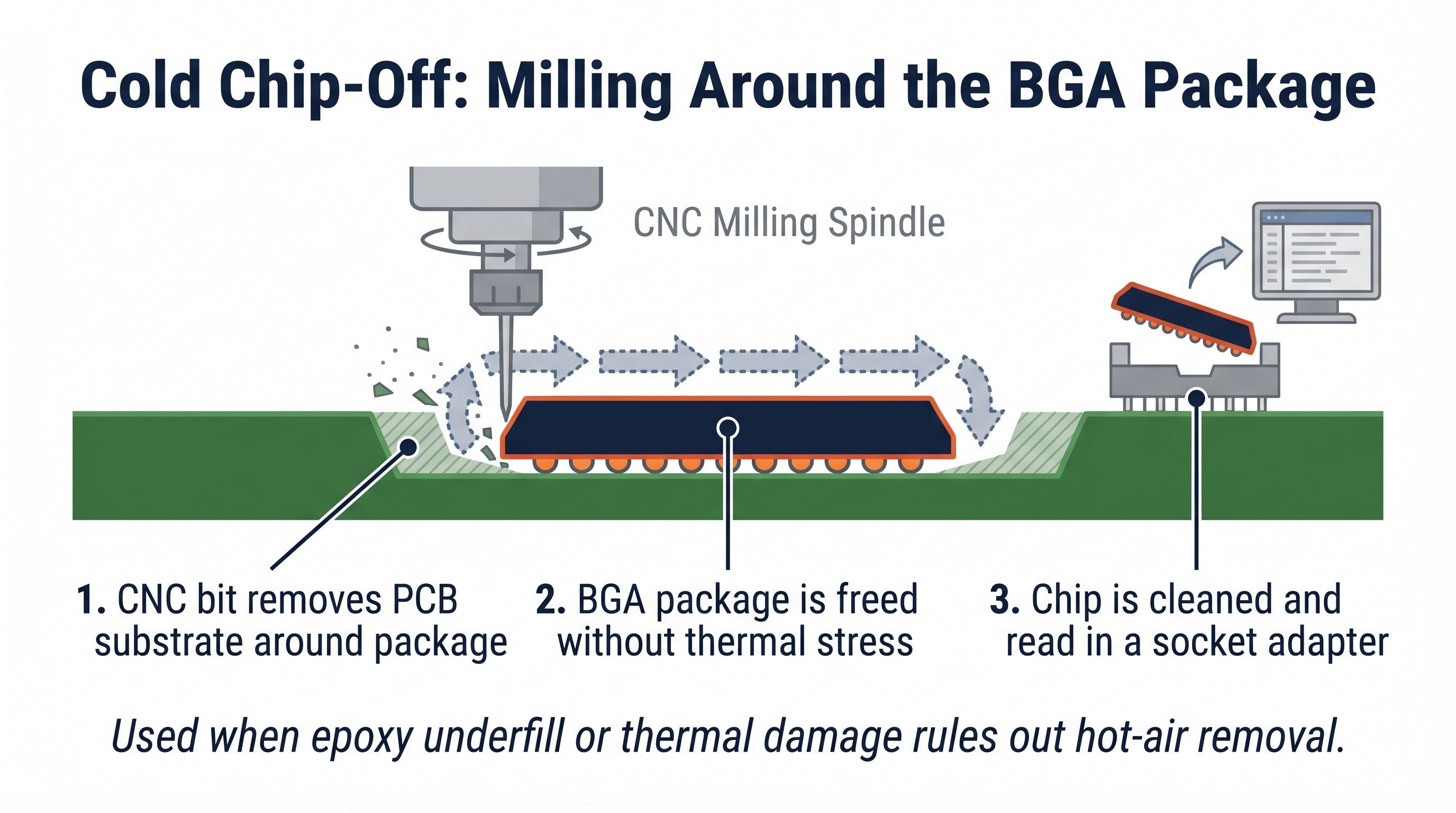
Figure 14.10: Cold chip-off conceptual cross-section. The CNC mill removes the PCB material around the chip rather than melting the solder underneath it.
Analyst Perspective
The decision between hot and cold removal is rarely close. If you can see epoxy underfill around the chip, or you have any reason to believe the device has been thermally stressed, cold removal is the only defensible choice. Hot-air on an underfilled chip is the single most common way labs destroy evidence in this discipline.
14.5 Why Modern Smartphones Resist These Methods
Every advanced physical acquisition method in this chapter delivers the same product: a raw image of the storage medium. On a modern Apple or high-end Android device, that image is encrypted with keys the examiner cannot reach.
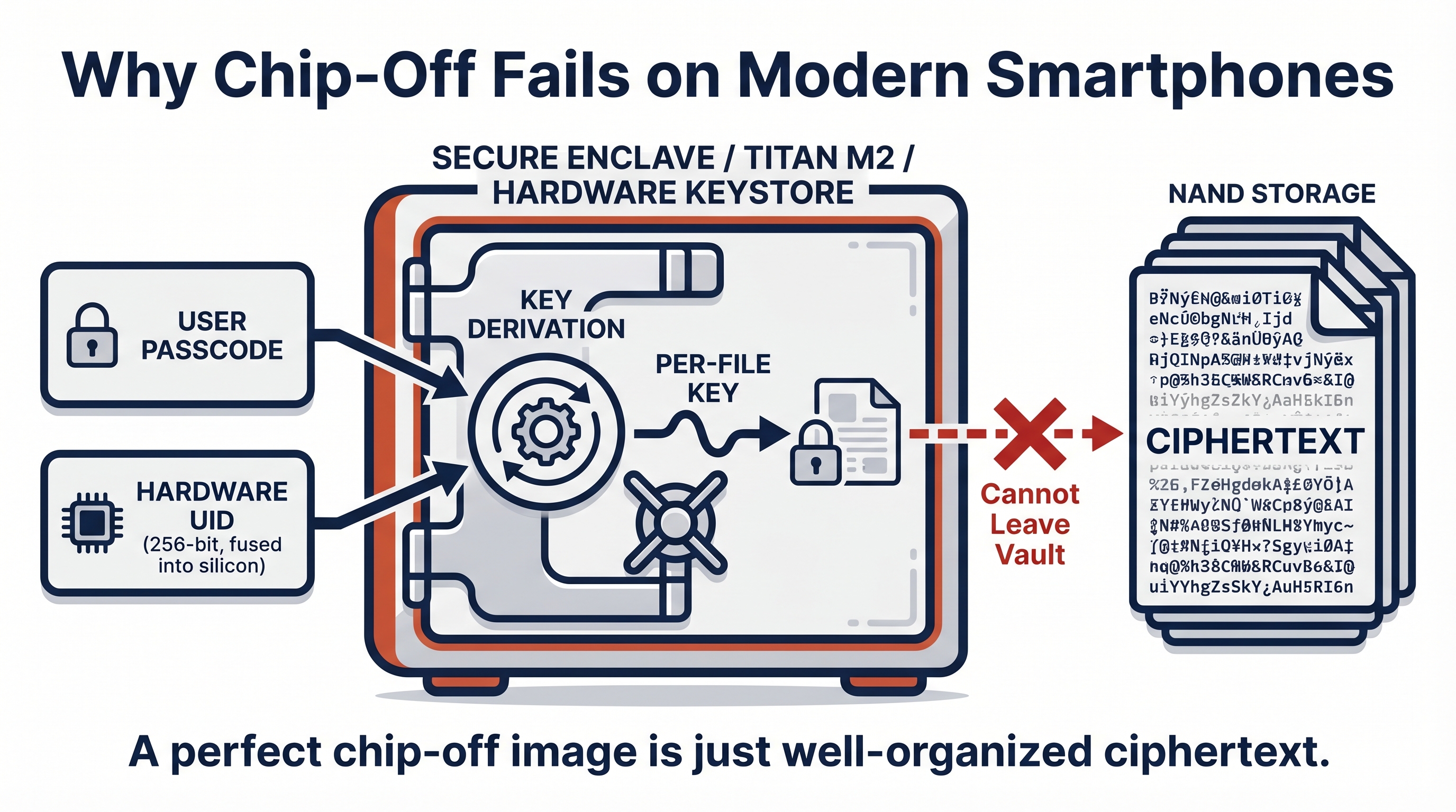
Figure 14.11: Hardware-backed key derivation. The user passcode and a chip-bound UID combine inside the security core to produce file keys that never leave the silicon. A chip-off NAND dump returns ciphertext only.
Apple's Secure Enclave Processor, introduced with the A7 system-on-chip and present in every iPhone since the 5s, is a separate processor with its own boot ROM, firmware, and isolated memory. The SEP holds the device's Unique Identifier (UID), a 256-bit key fused into the silicon at manufacture. The UID never leaves the SEP. File-level encryption keys for user data are derived by combining the user's passcode with the UID inside the SEP, then released to main memory only when the device is unlocked. As Chapter 11 covered in detail, this means a chip-off image of an iPhone's NAND contains file contents encrypted with keys that exist only inside a chip the examiner did not extract.
Android implements a comparable model through hardware-backed keystores. Google's Titan M2 (in Pixel 6 and later) and Samsung's equivalent secure elements perform key derivation in dedicated silicon. File-Based Encryption, mandatory since Android 10, encrypts each user's directories with per-file keys derived from the user credential and a hardware-bound key. Samsung Knox adds a measured boot chain and a one-way "warranty bit" that records tampering. As Chapters 9 and 10 explained, the practical effect for chip-off is identical to iOS. The dump is ciphertext.
The brute-force math reinforces the point. A six-digit numeric passcode has one million possible values. Hardware key derivation deliberately rate-limits each guess so that attempting all one million takes years on the device itself. Removing the chip strips the rate limit but also strips access to the UID, so offline attack is mathematically impossible without breaking AES, which no public technique does.
Warning
Do not let this section convince you that physical acquisition is obsolete. It convinces you only that physical acquisition is the wrong tool for current flagship smartphones. On an IoT device with no hardware key store, on a drone storing flight logs in plaintext, or on a damaged feature phone, the same techniques still produce readable evidence.
14.6 Where These Methods Still Pay Off
Physical acquisition remains a routine, high-yield technique across an entire ecosystem of devices that were never built with hardware-backed encryption. Cost, power budget, time-to-market, and the absence of a regulatory push have all kept these device classes on plaintext or weakly protected storage. The following are the device classes where labs see the most consistent value in 2026.
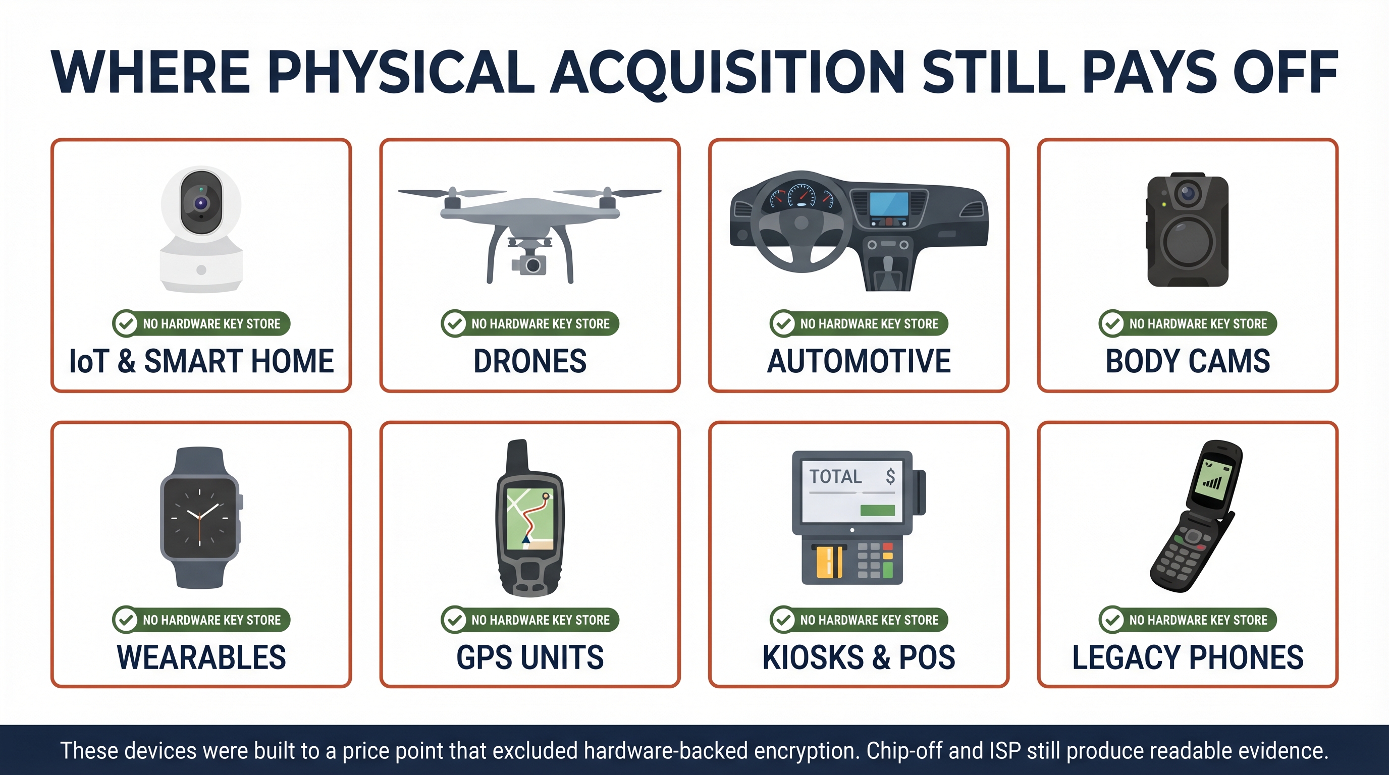
Figure 14.12: The device classes where physical acquisition remains the highest-yield approach in 2026. Each shares the same root cause: no hardware-backed key store protecting at-rest data.
IoT and smart-home devices. Smart locks, IP cameras, video doorbells, smart speakers, and home automation hubs typically run a stripped-down Linux or real-time operating system (RTOS) on a system-on-chip with eMMC or raw NAND storage. Encryption, when present at all, is often a transport-layer concern rather than a storage concern. Chip-off and ISP routinely yield Wi-Fi credentials, user account tokens, motion-event timelines, and cached audio or video.
Drones and unmanned aerial vehicles. Consumer and prosumer drones, particularly the DJI line, store flight logs, GPS tracks, telemetry, and frequently media on internal flash. Damage from crashes is common, which is exactly the case where ISP or chip-off is the only viable path. Flight logs are valuable in trespass, surveillance, and accident investigations.
Automotive infotainment and telematics. Head units, telematics control units (TCUs), and event data recorders carry navigation history, paired phone identifiers, contact and call logs synchronized from paired phones, and in some cases driver-behavior data. Many of these boards use industrial-grade chips with epoxy underfill, which is why cold chip-off appears more often in automotive work than in any other context.
Body-worn cameras and dashcams. Public-safety body cameras and consumer dashcams are typically large flash-storage devices in rugged housings. When a camera is damaged in an incident, chip-off may be the only way to recover the footage from the period of interest.
Fitness wearables and health trackers. Sleep, heart rate, GPS, and step data on smartwatches and fitness bands often live on internal flash with minimal protection. These artifacts have been useful in homicide and missing-person investigations as corroborating timelines.
GPS units and navigation devices. Standalone GPS units (Garmin, TomTom, marine and aviation chartplotters) store waypoints, route history, and in some cases voice annotations. Older units in particular respond well to ISP and chip-off.
Kiosks, point-of-sale terminals, and ATMs. Retail and financial endpoint hardware often runs aging embedded operating systems on commodity flash. Skimming, internal-fraud, and tampering investigations regularly rely on physical acquisition to capture transaction logs and tampering artifacts.
Legacy and feature phones. Pre-smartphone handsets continue to surface in elder-fraud, human-trafficking, and cold-case investigations. Many feature phones never used encryption at all. JTAG and chip-off remain the standard recovery path.
Analyst Perspective
When a non-smartphone device arrives in your lab, the right first question is not "can I chip this off." It is "does this device have a hardware key store, and if so what does it protect." For most of the device classes above, the honest answer is "none" or "transport keys only." That answer is what makes physical acquisition still worth your bench time.
14.7 Documentation, Validation, and Reporting
Invasive acquisition raises the documentation bar. The device leaves the lab in a different physical state than it arrived, and the examiner must be able to defend every alteration. Five practices distinguish defensible work from work that will be excluded.
Photographic documentation at every stage. Photograph the device on receipt, after disassembly, after shielding removal, before any soldering or milling, after each rework step, and with the chip seated in its reader. Most labs maintain a standard photo template so no step is skipped. These photographs become exhibits.
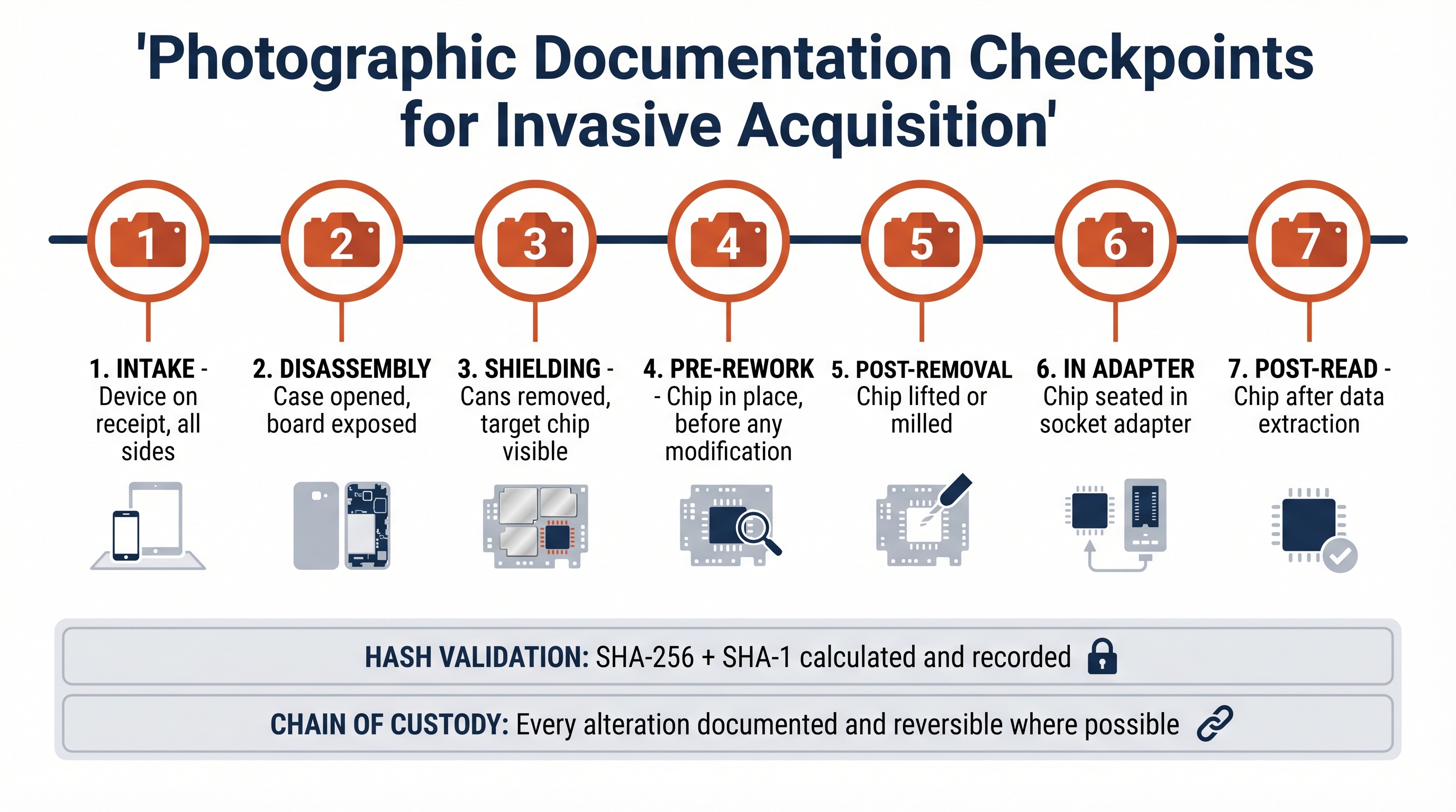
Figure 14.13: The seven photographic checkpoints that make invasive acquisition defensible in court. Skipping any of these creates an evidentiary gap that opposing counsel can exploit.
Figure 14.14: X-ray view of BGA solder joints. Forensic labs use X-ray imaging both to confirm rework quality and to add an additional verification artifact to the documentation record. Image by DJGB, public domain via Wikimedia Commons.
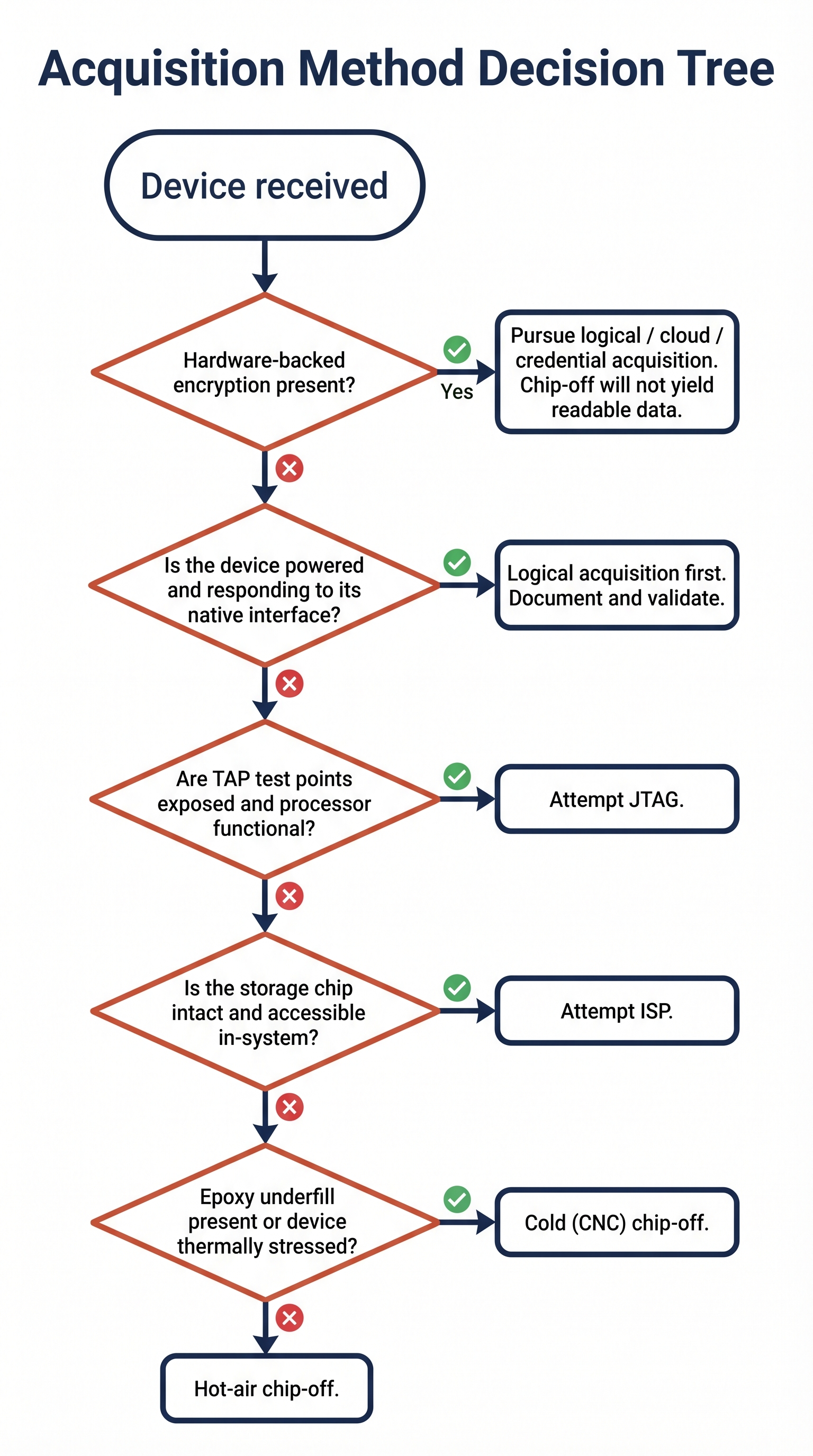
Figure 14.15: A working decision tree for selecting an acquisition method. The first question is always whether hardware-backed encryption will defeat the effort regardless of technique chosen.
Hash validation of the dump. As soon as the raw image is read, calculate at least two independent cryptographic hashes (typically SHA-256 and SHA-1 for legacy compatibility) and record them in the case notes. Re-hash the working copy before any analysis. Any later challenge to the integrity of the image is answered by re-running the hash.
Flash Translation Layer (FTL) and ECC awareness. Raw NAND images carry the chip's internal accounting structures, including wear-leveling tables, bad-block markers, and Error-Correction Code (ECC) parity. Parsing tools must be configured for the chip's FTL; otherwise the image will be misinterpreted as fragmented or corrupt. eMMC and UFS images present a logical view that hides most of this, but spare areas may still need explicit handling.
Parsing and interpretation tooling. The major commercial platforms (Cellebrite Physical Analyzer, Magnet AXIOM, MSAB XRY, X-Ways Forensics) all accept raw eMMC and UFS images and parse common filesystems automatically. Open-source workflows using Autopsy, Sleuth Kit, and ReclaiMe are viable for filesystems they support. For obscure embedded filesystems (YAFFS2, JFFS2, UBIFS), the examiner may need to build the parsing chain manually.
Court-facing reporting. Reports for invasive acquisition should explicitly identify the technique used, the justification for choosing it over less invasive alternatives, the equipment make and model, the examiner's training and certification, the photographs taken, and the hash values produced. The report should also identify any alterations to the device that are not reversible, so the chain of custody clearly reflects the device's post-examination state.
Warning
The single most common reporting failure in chip-off work is omitting the "less invasive alternatives considered" section. A defense expert who can show that ISP would have worked, but was skipped, can frame a chip-off as gratuitous destruction of evidence. Document the decision tree, not just the destination.
Acquisition Method Reference Matrix
The following matrix consolidates the four techniques covered in this chapter for use as a quick-reference and study aid.
| Attribute | JTAG | ISP | Hot Chip-Off | Cold Chip-Off |
|---|---|---|---|---|
| Access point | Processor TAP pads | eMMC/UFS data pads | Removed chip in socket | Removed chip in socket |
| Invasiveness | Low (test points) | Moderate (micro-solder) | High (chip removed via heat) | Highest (PCB milled away) |
| Reversibility | Fully reversible | Largely reversible | Not reversible | Not reversible |
| Equipment cost band | $1k to $5k | $1k to $5k | $5k to $15k | $25k to $75k+ |
| Skill floor | Moderate | High (micro-soldering) | High (BGA rework) | Highest (CNC operation) |
| Time on bench | 2 to 8 hours | 2 to 6 hours | 4 to 12 hours | 8 to 24 hours |
| Risk to device | Low | Moderate | High | High |
| Tolerates dead processor | No | Yes | Yes | Yes |
| Tolerates damaged board | Limited | Limited | Yes | Yes |
| Best fit | Lower-end Android, embedded boards, legacy phones with TAPs exposed | Mid-range and older smartphones, IoT, drones with intact boards | Damaged devices, IoT/wearables, consumer-grade BGA targets | Automotive, industrial, epoxy-underfilled, or thermally stressed targets |
Putting It Together
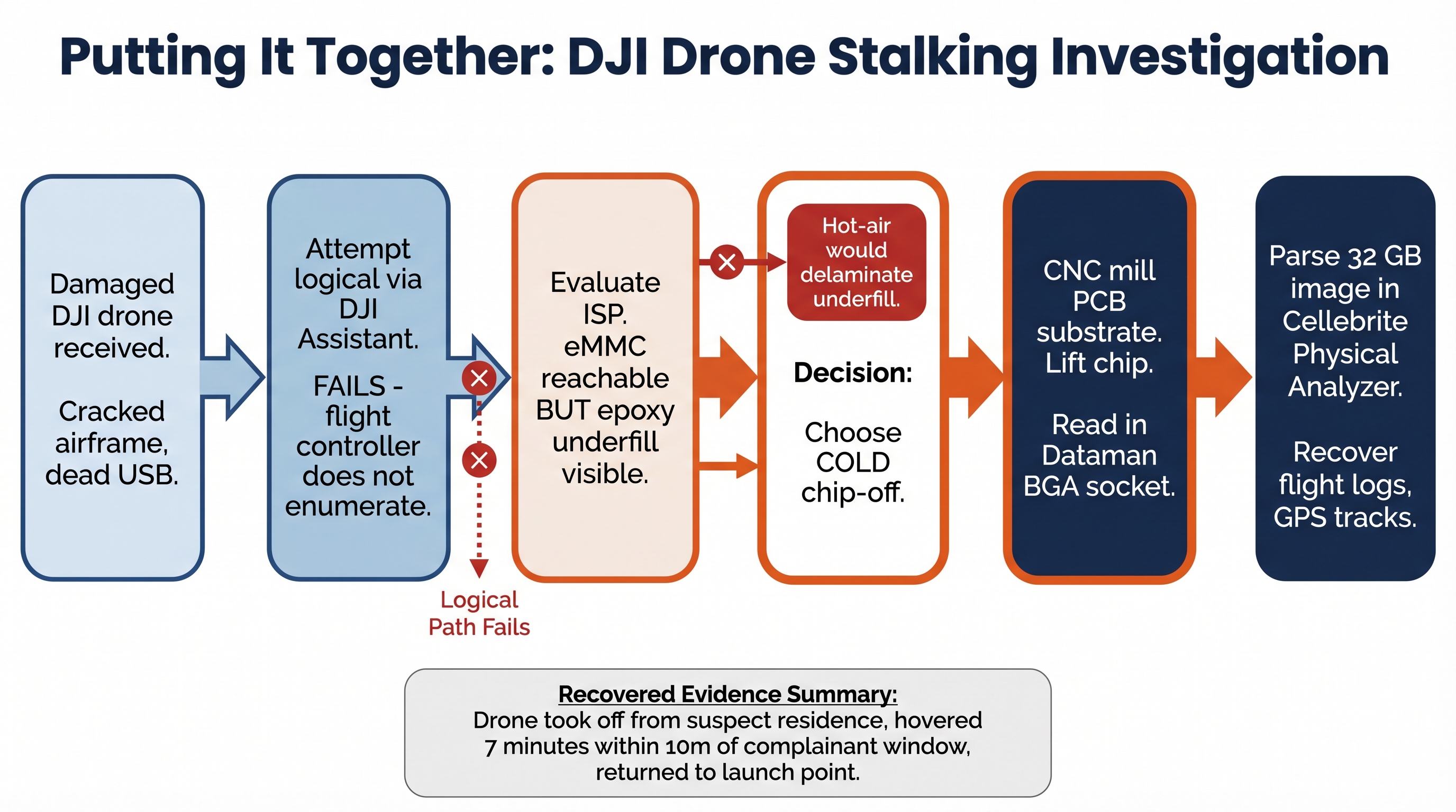
Figure 14.16: The decision flow for the DJI drone scenario walked through below. Each rejected option becomes a documented justification in the final report.
A small-municipality police agency arrives at the lab with a DJI consumer drone recovered from the rear yard of a residence under investigation for a stalking complaint. The drone's airframe is cracked, the camera gimbal is hanging by its ribbon cable, and one motor arm has separated. A neighbor's doorbell camera captured the drone hovering over the complainant's bedroom window for several minutes the previous night. The agency wants flight logs, GPS tracks, and any captured media.
The examiner begins with the least invasive option, attempting to power the drone and connect it to DJI Assistant on a forensic workstation. The drone's flight controller does not enumerate. Visual inspection under the stereo microscope reveals impact damage to the USB pads on the controller PCB. Attempting to re-establish those pads would risk further board damage and would not address the underlying question of whether the controller itself is functional.
The examiner moves to ISP. A pinout for this DJI flight controller's eMMC is documented in the lab's internal pinout archive (DJI shares enough hardware lineage across consumer models to make this practical). However, when the shielding can is removed, the eMMC package is visibly secured with a black epoxy underfill, consistent with DJI's vibration-hardening design choices on this model.
The decision tree now points firmly to cold chip-off. Hot-air would risk delaminating the underfilled package, and the case warrants the destruction of the controller given the felony stalking charge under consideration. The examiner photographs the board, mills away the PCB substrate around the eMMC package using the lab's CNC rig with a 0.3 mm bit on a documented program, lifts the package, cleans the underside ultrasonically, and seats the chip in a Dataman BGA socket. The eMMC reads cleanly to a 32 GB raw image. SHA-256 and SHA-1 hashes are calculated and recorded.
Parsing the image in Cellebrite Physical Analyzer surfaces the FAT32 partition the controller uses for flight logs, plus a separate region holding cached telemetry. The flight logs show the drone took off from a GPS coordinate matching the suspect's residence, flew a path consistent with the doorbell camera footage, hovered for seven minutes within ten meters of the complainant's bedroom window, and returned to the launch point. No media files are present (the drone's media is stored on a removed SD card not recovered with the airframe).
The report documents the decision to skip USB acquisition (hardware damage), the decision to skip ISP (epoxy underfill), the decision to use cold rather than hot chip-off (same), the equipment and program used, the hash values, and the parsed artifacts. The drone controller is preserved as an exhibit in its post-examination state.
Chapter Summary
- Advanced physical acquisition covers three techniques (JTAG, ISP, and chip-off) that bypass the operating system and read storage at the hardware level.
- JTAG uses the IEEE 1149.1 debug interface to drive the processor into reading storage on the examiner's behalf. It is fast to attempt but depends on a working processor and on TAP pinouts that modern flagships have removed.
- ISP solders directly to eMMC or UFS data pads, bypassing the processor. It is the modern workhorse for in-board acquisition where the storage chip is intact.
- Chip-off removes the storage chip entirely. Hot-air removal uses a controlled thermal cycle and suits most consumer-grade BGA targets. Cold (mechanical) removal uses CNC milling and is reserved for epoxy-underfilled, thermally stressed, or stacked packages.
- Modern Apple and high-end Android smartphones resist these methods because file encryption keys are derived inside hardware-isolated security cores (Secure Enclave, Titan M2, equivalent) that the examiner cannot extract. Raw dumps from these devices are unreadable ciphertext.
- Physical acquisition remains highly productive on IoT devices, drones, automotive infotainment, body cameras, fitness wearables, GPS units, kiosks and POS terminals, and legacy feature phones, where hardware-backed encryption is absent.
- Defensible invasive acquisition requires photographic documentation at every stage, dual-hash validation, FTL and ECC awareness during parsing, and a report that explicitly justifies the choice of technique against less invasive alternatives.
This chapter closes the CFS280 acquisition arc. You began the course at the logical and cloud layers, worked through filesystem and OS-specific examination, and now hold the analytical framework for the entire spectrum down to silicon. The same disciplined decision tree applies regardless of where on that spectrum you begin: identify the device's protections, choose the least invasive technique that will produce the evidence you need, document every step, and validate everything you report.
Image Credits
This chapter draws on photographs sourced from Wikimedia Commons under open licenses, and on instructional diagrams generated for this course using Google's Gemini image generation model. Per the terms of the Creative Commons Attribution-ShareAlike licenses on the photographs, derivative works incorporating those images must be released under a compatible license.
Photographs and Diagrams (Wikimedia Commons)
- Figure 14.2: "HY27UH088G2M" by Mister rf, licensed under CC BY-SA 4.0. Source: Wikimedia Commons.
- Figure 14.4: "JTAG TAP Controller State Diagram" by Rudolph H, released under copyrighted free use. Source: Wikimedia Commons.
- Figure 14.5: "Samsung eMMC chip KLMCG8GEAC-B001" by Toniperis, licensed under CC BY-SA 4.0. Source: Wikimedia Commons.
- Figure 14.7: "Cross section of a BGA chip package" by TubeTimeUS, licensed under CC BY-SA 4.0. Source: Wikimedia Commons.
- Figure 14.9: "Desoldering with hot air" by Aisart, licensed under CC BY-SA 3.0. Source: Wikimedia Commons.
- Figure 14.14: "14×14 BGA board's x-ray" by DJGB, released into the public domain. Source: Wikimedia Commons.
Instructional Diagrams (AI-Assisted)
Figures 14.1, 14.3, 14.6, 14.8, 14.10, 14.11, 14.12, 14.13, 14.15, and 14.16 were drafted using Google's Gemini image generation model from prompts authored for this chapter. Concept, structure, technical content, and labeling were specified by the author; the model rendered the visual layout. All AI-generated figures were reviewed for technical accuracy before inclusion. These diagrams are released under the same license as the chapter text.